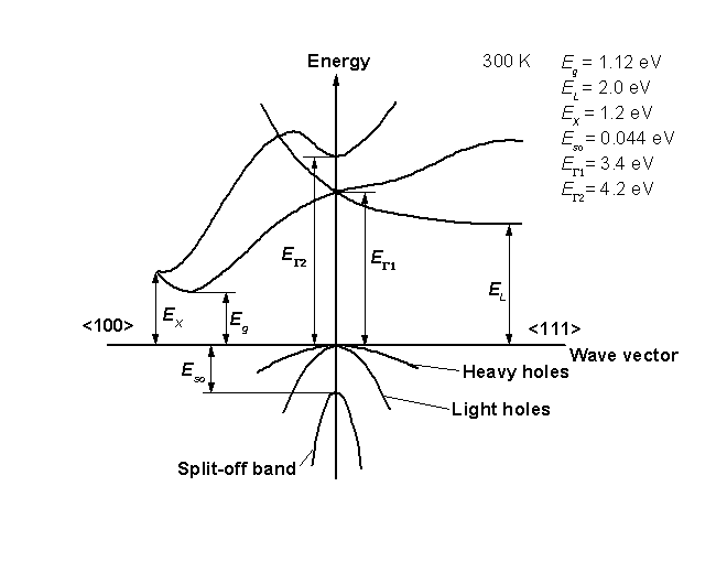
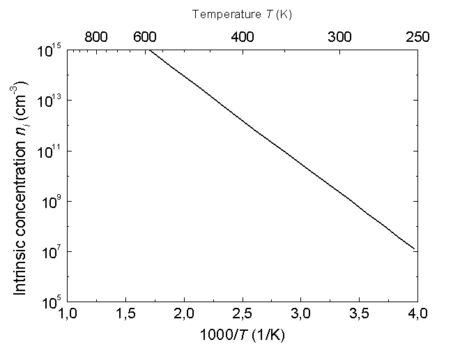
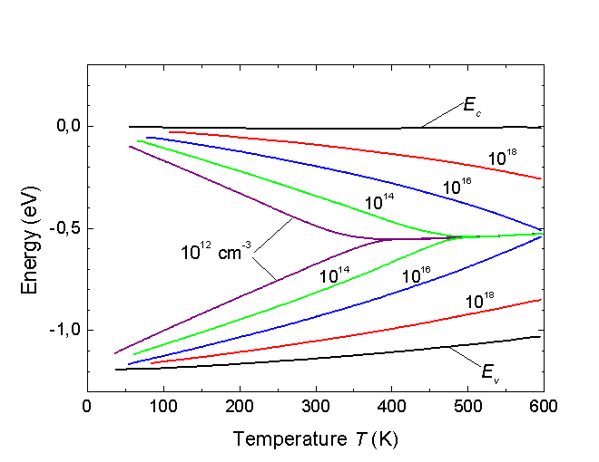
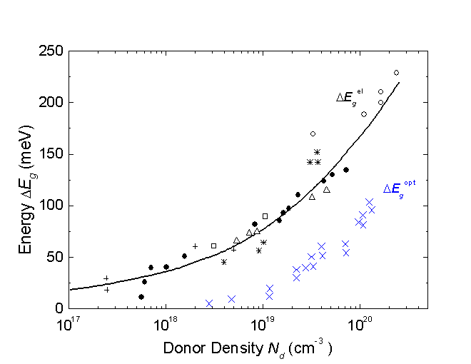
Crystal structure,Group of symmetry,Number of atoms in 1 cm3,Auger recombination coefficient Cn, Auger recombination coefficient Cp, Debye temperature, Density, Dielectric constant, Effective electron mass,Effective electron mass,Effective hole mass,Effective hole mass,Electron affinity, Lattice constant, Optical phonon energy, Energy gap, Energy separation, Energy spin-orbital splitting, Intrinsic carrier concentration, Intrinsic resistivity, Effective conduction band density states,Effective valence band density of states, Band structure of Si at 300 K,Temperature dependence of the energy gap,Temperature dependence of the energy gap,Temperature dependence of the direct band gap, Intrinsic carrier concentration,Effective density of states in the conduction band,Effective density of states in the valence band,The temperature dependence of the intrinsic carrier concentration.(Shur [1990]),Fermi level versus temperature for different concentrations of shallow donors and acceptors,(Grove [1967]),Dependence of the Energy Gap on Hydrostatic Pressure,Electrical and optical energy gap narrowing versus donor doping density. (Van Overstaeten and Mertens [1987]),For 1 E17 ≤ N ≤ 3 E17 cm-3,ΔEgel ~ 3.5E-8·Nd1/3 (eV); (Nd in cm-3),Effective Masses of Electrons, Effective Masses of Holes, Ionization energies of shallow DONORS (eV),Ionization energies of shallow ACCEPTORS (eV),Deep Levels Impurities,*Position in the Forbidden group,a - acceptor, d - donor SiO2 color chart for thermally grown silicon dioxide, HTE Labs provides process specialties wafer foundry, thin film vacuum deposition services, applied thin film processing for analog and mixed signal bipolar manufacturing processes, Analog CMOS wafer foundry, R&D support, research and development support for microelectronics and process specialties wafer Fab processing to customers from semiconductors and microelectronics industry. Bipolar wafer foundry includes the following processes: 20V bipolar process,45V bipolar process,75V bipolar process,25V super-beta bipolar process and high voltage dielectric isolated bipolar processes. R&D support is provided in the following fields of microelectronics: test and measurement, medical instrumentation, industrial process control and communications, thin film active and passive components technologies, flip chip technology (TiW/Cu/Cu/SnPb), MEMS technology, smart sensor technologies (inertial, pressure, temperature, gas and smoke detectors), optoelectronic technologies and components, discrete and integrated circuits technology development for special applications, LiNbO3 applications including SAW, Ti diffusion, light wave guides and Mach-Zender light modulators. Specialty wafer Fab processing: epi deposition, epitaxy, SiGe, epi, diffusion and oxidation, ion implant, LPCVD nitride, PECVD nitride Si3N4, SiO2, platinum silicidation, photo-lithography, plasma etching, silicon micro-machining with KOH anisotropic etch, backside sputter depositions of Ti/Ni/Ag, gold deposition, gold alloy, lift off processes, Ti/Pt/Au lift off process, sputter depositions of thin film resistors : SiCr, NiCr, TaN2, silicon wafers back grind and polish followed by tri-metal backside sputter depositions, gold backside sputter depositions and alloy : gold electroplating and gold bump, wafer probing, dicing services, wafer saw, package development, solid via packages, packaging and test services, failure analysis services, SEM, scanning electron microscopy, ellipsometer measurements, four point probe measurements.
 

Si - Silicon physical properties at 300K
Collection of articles, abstracts, technical notes, letters, links, publications
HTE Labs  


PUBLISHER-AUTHOR INFORMATION  
   
IOFE PHYSICO-TECHNICAL INSTITUTE
http://www.ioffe.rssi.ru
 
Crystal structure  Diamond
Group of symmetry Oh7-Fd3m
Number of atoms in 1 cm3 5·E22
Auger recombination coefficient Cn 1.1E-3cm6s-1
Auger recombination coefficient Cp 3E-31cm6s-1
Debye temperature 640 K
Density 2.329 g cm-3
Dielectric constant 11.7
Effective electron mass ml=0.98mo
Effective electron mass mt=0.19mo
Effective hole mass mh=0.49mo
Effective hole mass mlp=0.16mo
Electron affinity 4.05 eV
Lattice constant 5.431 A
Optical phonon energy 0.063 eV
Energy gap 1.12 eV
Energy separation 4.2 eV
Energy spin-orbital splitting 0.044 eV
Intrinsic carrier concentration 1·E10 cm-3
Intrinsic resistivity  3.2·E5 Ω·cm
Effective conduction band density states 3.2·E19 cm-3
Effective valence band density of states 1.8·E19 cm-3
Band structure of Si at 300 K.
Eg = 1.12 eV
EL = 2.0 eV
EX = 1.2 eV
Eso = 0.044 eV
EΓ1 = 3.4 eV
EΓ2 = 4.2 eV

[click image to enlarge]
Temperature dependence of the energy gap Eg = 1.17 - 4.73·10-4·T2/(T+636) (eV)
where T is temperature in degrees K.
Temperature dependence of the direct band gap EΓ2 = 4.34 - 3.91·10-4·T2/(T+125) (eV)
Intrinsic carrier concentration ni=(Nc·Nv )1/2·exp(-Eg/(2kBT])
Effective density of states in the conduction band Nc=4.82·1015·M·(mc/mo)3/2·T3/2 = 4.82·1015·M·(mcd/mo)3/2·T3/2 (cm-3), or
Nc=6.2·1015·T3/2 (cm-3),
M = 6 is the number of equivalent valleys in the conduction band.
mc = 0.36mo is the effective mass of the density of states in one valley of conduction band.
mcd = 1.18mo is the effective mass of the density of states.
Effective density of states in the valence band Nv = 3.5·1015·T3/2 (cm-3)
The temperature dependence of the intrinsic carrier concentration.
(Shur [1990]).

[click image to enlarge]
Fermi level versus temperature for different concentrations of shallow donors and acceptors.
(Grove [1967]).

[click image to enlarge]
Dependence of the Energy Gap on Hydrostatic Pressure Eg=Eg(0)-1.4·10-3P (eV)
Electrical and optical energy gap narrowing versus donor doping density. (Van Overstaeten and Mertens [1987]) For 1 E17 ≤ N ≤ 3 E17 cm-3
ΔEgel ~ 3.5E-8·Nd1/3 (eV); (Nd in cm-3).

[click image to enlarge]
Effective Masses of Electrons: The surfaces of equal energy are ellipsoids.
ml= 0.98mo
mt= 0.19mo
Effective mass of density of states mc = 0.36mo
There are 6 equivalent valleys in the conduction band.
mcc= 0.26mo
Effective Masses of Holes Heavy mh = 0.49mo
Light mlp = 0.16mo
Split-off band mso = 0.24mo
Effective mass of density of states mv = 0.81mo
Ionization energies of shallow DONORS (eV) As = =0.054; P = 0.045;  Sb = 0.043
Ionization energies of shallow ACCEPTORS (eV) Al = 0.072; B = 0.045;  Ga = 0.074;  In = 0.157
Deep Levels Impurities *Position in the Forbidden group
a - acceptor, d - donor.
Impurity Type Position* σn (cm2) σp(cm2)
Au n Ev+ 0.35 eV 1E-15 3.5 E-15
a Ec  -0.55 eV 8E-17 9.0 E-15
Cu d  Ev+ 0.24 eV   3.5 E-20
a  Ev+ 0.37 eV    
a Ev+ 0.52 eV    
Fe d Ev+ 0.39 eV   2.0 E-17
Ni a Ec- 0.35 eV 7E-12  
a Ev+ 0.23 eV    
Pt d Ev+ 0.32 eV 5E-14 ~ 1E-15
a Ev+ 0.36 eV    
a Ec- 0.25 eV    
Zn a Ev+ 0.32 eV 1E-15 1E-13
a Ec- 0.50 eV 1E-19 1E-13
   
  <Previous page - Page 1 - Next page >

Home>Application Notes> Last updated: July 06, 2009

HTE LABS Tel:(408)758-8691 Fax:(408)986-8027

©1990-2024 HTE LABS All rights reserved. No material from this site may be used or reproduced without permission.